- 您现在的位置:买卖IC网 > Sheet目录326 > FLS2100XS (Fairchild Semiconductor)IC CTLR FPS HALF BRIDG LCC 9-SIP
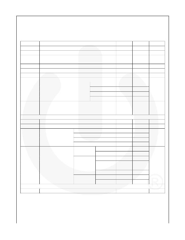
Absolute Maximum Ratings
Stresses exceeding the absolute maximum ratings may damage the device. The device may not function or be
operable above the recommended operating conditions and stressing the parts to these levels is not recommended. In
addition, extended exposure to stresses above the recommended operating conditions may affect device reliability. The
absolute maximum ratings are stress ratings only. T A =25 ° C unless otherwise specified.
Symbol
V DS
LV CC
Parameter
Maximum Drain-to-Source Voltage (V DL -V CTR and V CTR -PG)
Low-Side Supply Voltage
Min.
500
-0.3
Max.
25.0
Unit
V
V
HV CC to V CTR High-Side V CC Pin to Low-Side Drain Voltage
-0.3
25.0
V
HV CC
V AR
V CS
V RT
dV CTR /dt
High-Side Floating Supply Voltage
Auto-Restart Pin Input Voltage
Current-Sense (CS) Pin Input Voltage
R T Pin Input Voltage
Allowable Low-Side MOSFET Drain Voltage Slew Rate
-0.3
-0.3
-5.0
-0.3
525.0
LV CC
1.0
5.0
50
V
V
V
V
V/ns
FLS2100XS
12.0
P D
Total Power Dissipation
(3)
FLS1800XS
FLS1700XS
11.7
11.6
W
FLS1600XS
11.5
Maximum Junction Temperature
Recommended Operating Junction Temperature
T J
T STG
Storage Temperature Range
(4)
(4)
-40
-55
+150
+130
+150
° C
° C
MOSFET Section
V DGR
V GS
Drain Gate Voltage (R GS =1M Ω )
Gate Source (GND) Voltage
FLS2100XS
500
±30
32
V
V
I DM
Drain Current Pulsed
(5)
FLS1800XS
FLS 1700XS
23
20
A
FLS 1600XS
18
FLS2100XS
T C =25 ° C
T C =100 ° C
10.5
6.5
I D
Continuous Drain Current
FLS1800XS
FLS 1700XS
T C =25 ° C
T C =100 ° C
T C =25 ° C
T C =100 ° C
7.0
4.5
6.0
3.9
A
Package Section
FLS 1600XS
T C =25 ° C
T C =100 ° C
4.5
2.7
Torque
Recommended Screw Torque
5~7
kgf·cm
Notes:
3. Per MOSFET when both MOSFETs are conducting.
4. The maximum value of the recommended operating junction temperature is limited by thermal shutdown.
5. Pulse width is limited by maximum junction temperature.
? 2010 Fairchild Semiconductor Corporation
FLS-XS Series ? Rev.1.0.0
4
www.fairchildsemi.com
发布紧急采购,3分钟左右您将得到回复。
相关PDF资料
FMD15.24G
1500W 24V DC-INPUT 48V RECTIFIER
FMP25.48G
2500W 48V AC-INPUT RECTIFIER
FND850-12DRG
FRONT END DC/DC 850W 12V
FND850-12RG
FRONT END DC/DC 850W 12V
FNR-5-12G
19" RACK FOR 5X 12V FRONT END
FPB
ADAPTER WALL FOLDING CLIP BR
FRJAE-418
CONN MOD RJ45 JACK R/A EMI FLTR
FS-9003
JTAG-BOOSTER FOR XSCALE 3.3V
相关代理商/技术参数
FLS-2182-26-12.00-.30-RED
功能描述:LAMP FLYING 5MM 26AWG 12"LD RED RoHS:否 类别:光电元件 >> 灯 - 白炽灯,氖灯 系列:- 标准包装:100 系列:- 颜色:透明 透镜样式/尺寸:圆形,带圆顶,5mm,T-1 3/4 引线型:小型凹槽 MSCP(平均球面烛光):0.3 额定电压:60V 其它名称:913.4005913.4005-ND
FLS-2B01-001
制造商:Dialight 功能描述:SINGLE,BLU,120 VAC,C1,D2
FLS-2B01-005
制造商:Dialight 功能描述:BLUE 120V SGL C1D2 JNCTN HSG
FLS-2B02-001
制造商:Dialight 功能描述:FXTR SGL BLU 240 V CLS1, DV 2
FLS-2B09-001
制造商:DIALIGHT 制造商全称:Dialight Corporation 功能描述:SafeSit? LED Signaling for Hazardous Locations
FLS-2G01-001
制造商:Dialight 功能描述:SINGLE,GRN,120 VAC,C1,D2
FLS-2G02-001
制造商:Dialight 功能描述:SINGLE,GRN,240 VAC,C1,D2
FLS-2G09-001
制造商:DIALIGHT 制造商全称:Dialight Corporation 功能描述:SafeSit? LED Signaling for Hazardous Locations
